| FEATURES |
APPLICATIONS |
Bipolar Silicon Transistors
- BARE DIE
|
High reliability bare die
Gold metallization
RoHS compliant, Lead Free
Compatible with chip and wire assemblies
Available as lateral or vertical PNP tansistor
|
Chip on Board
System in package SIP
Hybrid Circuits
Automotive, Biotechnology, Computers, Military, Medical, MEMS, Optoelectronics, Space, Telecommunications
Smart Cards, RFID, PDA, Laptops, Mobile phones
|

|
| BIPOLAR SILICON TRANSISTORS PNP - PRODUCT DESCRIPTION |
Semiconix Semiconductor PNP low power transistors series are designed to be used in a wide variety of digital and
analog functions, including amplification, switching, voltage regulation, signal modulation, and oscillators. Semiconix Semiconductor
PNP low power transistors series are available as discrete devices or as part of a hybrid integrated circuit
(complex devices) packaged in a very small area.
Semiconix Semiconductor transistors series may be used in many applications as hybrid Circuits, automotive, biotechnology, computers, military,
medical, MEMS, optoelectronics, space, telecommunications, smart cards, RFID, PDA, laptops and mobile phones.
PNP low power transistors remain the devices that excels in some applications, such as discrete circuit design,
due to the very wide selection of PNP low power transistors types available, and because of their high
transconductance and output resistance compared to MOSFETs. The PNP low power transistor is also the choice for
demanding analog circuits, especially for very-high-frequency applications, such as radio-frequency circuits for wireless systems. Because
of the known temperature and current dependence of the forward-biased base-emitter junction voltage, the PNP can
be used to measure temperature by subtracting two voltages at two different bias currents in a known ratio. Since base-emitter voltage varies
as the log of the base-emitter and collector-emitter currents, PNP low power transistors can also be used to
compute logarithms and anti-logarithms.
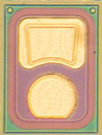
PNP low power transistors BD series are available in die form in two configurations, Vertical XXXX-BD or Lateral XXXXL-BD. In die form,
these products are ideal for high reliability hybrid circuits and multi chip module applications.
|
| HIGH RELIABILITY BARE DIE AND SYSTEM IN PACKAGE - SHORT APPLICATION NOTE |
|
COB (Chip on Board) and SiP (System-in-Package) are integrating proven mature products in bare die of mixed technologies i.e. Si, GaAs, GaN,
InP, passive components, etc that cannot be easily implemented in SOC (System-on-Chip) technology. COB and SiP have small size footprint,
high density, shorter design cycle time, easier to redesign and rework, use simpler and less expensive assembly process. For extreme applications
the bare die has to withstand also harsh environmental conditions without the protection of a package. KGD, Known Good Die concept is no longer
satisfactory if the die cannot withstand harsh environmental conditions and degrades. Standard semiconductor devices supplied by many manufacturers
in bare die are build with exposed aluminum pads that are extremely sensitive to moisture and corrosive components of the atmosphere. Semiconix
has reengineered industry standard products and now offers known good die for bare die applications with gold interconnection and well-engineered
materials that further enhance the die reliability. Semiconix also offers Silicon Printed Circuit Board technology with integrated passive
components as a complete high reliability SIP solution for medical, military and space applications. See AN-SMX-001
|
| DISCRETE SEMICONDUCTORS MANUFACTURING PROCESS |
|
Discrete semiconductors are manufactured using Semiconix in house high reliability semiconductor manufacturing processes. All semiconductor
devices employ precision doping via ion implantation, silicon nitride junction passivation, platinum silicided contacts and gold interconnect
metallization for best performance and reliability. MNOS capacitors, Tantalum Nitride TaN or Sichrome SiCr thin film resistors are easily
integrated with discrete semiconductors on same chip to obtain standard and custom complex discrete device solutions.
|
| Absolute Maximum Ratings * Ta = 25°C unless otherwise noted |
| Name |
Symbol |
Value |
Unit |
| Collector-Emitter Voltage |
VCEO |
30.00 |
V |
| Collector Current |
IC |
8.00 |
A |
| Collector Power Dissipation |
PC |
60.00 |
W |
| Electrical Characteristics* TC = 25°C unless otherwise noted |
| Name |
Symbol |
Test conditions |
Min. |
Typ. |
Max. |
Unit |
| Collector-Base Breakdown Voltage |
V(BR)CEO |
IC = 100mA, IB = 0 |
30.00 |
|
|
V |
| Collector-Cutoff Current |
ICBO1 |
VCB = 60V, IE = 0 |
|
|
10.00 |
mA |
| Emitter Cut-off Current |
IEBO |
VEB = 5V, IC = 0 |
|
|
100.00 |
mA |
| DC Current Gain |
hFE1 |
VCE = 5V, IC = 8A |
100.00 |
|
|
|
| DC Current Gain |
hFE2 |
VCE = 5V, IC = 10A |
80.00 |
|
|
|
| DC Current Gain |
hFE3 |
VCE = 5V, IC = 12A |
65.00 |
|
|
|
| Collector-Emitter Saturation Voltage |
VCE(sat)1 |
IC = 8A, IB = 0.4A |
|
|
1.00 |
V |
| Base-Emitter Saturation Voltage |
VBE (sat)1 |
IC = 8A, IB = 0.8A |
|
|
1.50 |
V |
| Current Gain - Bandwidth Product |
fT |
VCE = 10V, IC = 500mA |
25.00 |
|
|
MHz |
|
|
CROSS REFERENCE PARTS: Diode Inc. 2DA1774R
|
| GENERAL DIE INFORMATION |
| Substrate |
Thickness
[mils] |
Die size
[mils]
|
Bonding pads
|
Backside metallization
|
| Silicon |
8±1
|
±2
|
Pad metal is TiW/Au, 4µm±1 thick, 99.99% electroplated gold with TiW barrier. Custom metallization available upon request.
|
| P/N | Metal | Die attach process |
|---|
| -BD0 | Au/Si | Au/Si eutectic |
|---|
| -BD1 | Ti/Pd/Au | AuSn,AuGe |
|---|
| -BD2 | Ti/Pt/Au | AuSn,AuGe |
|---|
| -BD3 | Ti/Ni/Au | Soft Solder SAC |
|---|
| -BD4 | Ti/Pt/AuSn | AuSn eutectic |
|---|
|
| LAYOUT / DIMENSIONS / PAD LOCATIONS |
| Click to select image: |
LATERAL |
VERTICAL |
|
|
|
|

|
| SEMICONDUCTOR ASSEMBLY PROCESS - SHORT APPLICATION NOTE |
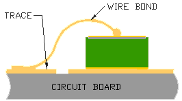
Semiconix standard bare die components are designed for thermosonic GOLD wire bonding and AuSi eutectic die attach. For AuSn or AuGe die
attach process, Ti/Pt/Au or Ti/Pd/Au are recommended backside metallization.
For soft solder die attach, backside metallization may be any of Ti/Ni/Au, Ti/Pt/Au, Ti/Pd/Au.
For silver filled conductive epoxy die attach, AuSi as well as Ti/Ni/Au, Ti/Pt/Au, Ti/Pd/Au may be used.
In general, after die attach, prior to wire bonding operation an oxygen RF plasma clean operation is recommended.
IMPORTANT NOTE: Aluminum wire should not be used with gold pads due to potential reliability problem known as purple plague. Same it applies
to Aluminum bonding pads with gold wire! In the transition from SnPb solder to lead free and RoHS compliant packaging and assembly processes
the reflow temperature has increased in some cases from 180°C to 220°C. This may cause an increase of the rate of formation of gold aluminum
intermetallic compounds that are brittle and are conducive to increased contact resistance and or bond failure. See Application note AN-SMX-000.
|
| STANDARD PRODUCTS ORDERING INFORMATION |
| VERSION |
SMX P/N |
WAFFLE PACKS |
QUANTITY |
U/P($) |
FILM FRAME |
MIN QUANTITY |
U/P($) |
| Lateral |
SMXD45H2AL-BD |
-WP |
10000 |
- |
-FF |
- |
- |
| Lateral |
SMXD45H2AL-BD |
-WP |
50000 |
- |
-FF |
- |
- |
| Vertical |
SMXD45H2A-BD |
-WP |
10000 |
|
-FF |
- |
|
| Vertical |
SMXD45H2A-BD |
-WP |
50000 |
|
-FF |
- |
|
|
PRICES - Listed prices are only for standard products, available from stock. Inventory is periodically updated. List prices for other quantities
and tolerances are available on line through Instant Quote. For standard products available from stock, there is a minimum line item order of
$550.00. No rights can be derived from pricing information provided on this website. Such information is indicative only, for budgetary use
only and subject to change by SEMICONIX SEMICONDUCTOR at any time and without notice.
|
|
LEAD TIMES - Typical delivery for standard products is 4-6 weeks ARO. For custom devices consult factory for an update on minim orders and lead times.
|
|
CONTINOUS SUPPLY - Semiconix guarantees continuous supply and availability of any of its standard products provided minimum order quantities are met.
|
|
CUSTOM PRODUCTS - For custom products sold as tested, bare die or known good die KGD, there will be a minimum order quantity MOQ. Dice are
100% functional tested, visual inspected and shipped in antistatic waffle packs. For high volume and pick and place applications, dice are
also shipped on film frame -FF. For special die level KGD requirements, different packaging or custom configurations, contact sales via
CONTACTS page.
|
|
SAMPLES - Samples are available only for customers that have issued firm orders pending qualification of product in a particular application.
|
|
ORDERING - Semiconix accepts only orders placed on line by registered customers. On line orders are verified, accepted and acknowledged by
Semiconix sales department in writing. Accepted orders are non cancelable binding contracts.
|
|
SHIPING - Dice are 100% functional tested, visual inspected and shipped in antistatic waffle packs. For high volume and pick and place
applications, dice are also shipped on film frame -FF.
|
|
DISCLAIMER - SEMICONIX has made every effort to have this information as accurate as possible. However, no responsibility is assumed by
SEMICONIX for its use, nor for any infringements of rights of third parties, which may result from its use. SEMICONIX reserves the right to
revise the content or modify its product line without prior notice. SEMICONIX products are not authorized for and should not be used within
support systems, which are intended for surgical implants into the body, to support or sustain life, in aircraft, space equipment, submarine,
or nuclear facility applications without the specific written consent.
|
| SEMICONIX SEMICONDUCTOR |
www.semiconix-semiconductor.com
Tel:(408)758-8694 Fax:(408)986-8027 |
SEMICONIX SEMICONDUCTOR |
| Last updated:July 03, 2009 |
Display settings for best viewing: |
Current display settings: |
| Page hits: 1 |
Screen resolution: 1124x864 |
Screen resolution:
|
| Total site visits:
|
Color quality: 16 bit |
Color quality:
bit |
| © 1990-2025 SEMICONIX SEMICONDUCTOR All rights reserved. No material from this site may be used or reproduced without permission. |
|